


Please Leave Us A Message
Privacy statement: Your privacy is very important to Us. Our company promises not to disclose your personal information to any external company with out your explicit permission.
製品情報
モデル: GD 015
輸送方法: Ocean,Air
お支払い方法の種類: L/C,T/T
インコタームズ: FOB,CFR,CIF
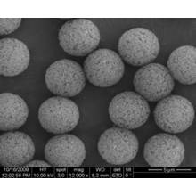
Nanomicro Techは、電子機器製造におけるマイクロエレクトロニクスパッケージング用の高品質のFaraBead®金メッキ粒子を提供しています。
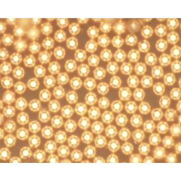
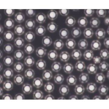
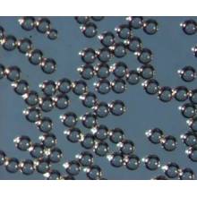
液晶ディスプレイ(LCD)の解像度を上げ、回路チップまたはモジュールの数を減らすと、集積回路の入力/出力(I / O)密度が増加し、相互接続バンプのサイズとピッチが非常に小さくなります。 FaraBead®Au粒子は導電性であり、通常はバインダーに分散して、微小電極の接続に使用される異方性導電フィルム(ACF)や異方性導電ペースト(ACP)などの異方性導電接着剤(ACA)材料を形成します。 FaraBead®Au導電性粒子は、優れたサイズ均一性、高導電性、適切な弾性、および金属層と樹脂コア間の強力な接着性を備えています。ファインピッチ電極の垂直接続用に特別に設計されたFaraBead®Au導電性粒子は、たとえば、LCDセルの製造における2つのガラスパネル間の相互接続に使用されます。

特徴
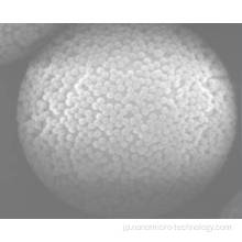
uコアとして単分散樹脂粒子、シェルとして金属金
u幅広いサイズの選択:3.0 µm − 10.0 µm (0.1 µm刻み)
uサイズと形状が均一、変動係数(CV)≤3.5 %
u優れた分散性、重複や凝集がない
u高い伝導信頼性のための適切な硬度
u抵抗が低く、高温多湿下での安定性が高い

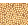
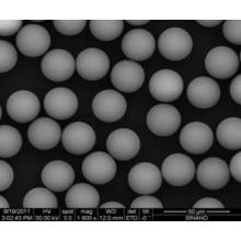
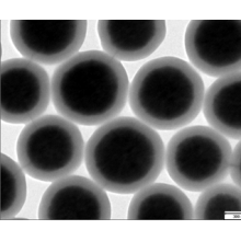
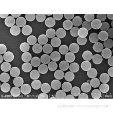
FaraBead®Au粒子の光学およびSEM顕微鏡写真
FaraBead®金
|
Product |
Diameter |
Increment |
CV |
K at 10% deformation* |
Metal thickness |
Metal content |
Application |
|
µm |
µm |
kgf / mm2 |
nm |
% |
|||
|
GD |
7.00–10.00 |
0.25 |
≤3.5% |
~450 |
100–150 |
25–35 |
LCD |
|
3.00–6.75 |
0.25 |
≤3.5% |
~500 |
100–150 |
30–40 |
||
|
GDL |
7.00–10.00 |
0.25 |
≤3.5% |
~250 |
100–150 |
25–35 |
ACF,ACP |
|
3.00–6.75 |
0.25 |
≤3.5% |
~300 |
100–150 |
30–40 |
* 10%の変形でのK値は、次の式で定義されます。
K =( 3 2 ) ∙ F ∙ S -3 / 2 ∙ R -1/2
ここで、 FとSは、それぞれ粒子の10%圧縮変形での荷重値( kgf )と圧縮変位( mm )を表し、 Rは粒子の半径( mm )を表します。
製品グループ : LCDスペーサーと導電性粒子 > 導電性粒子


Privacy statement: Your privacy is very important to Us. Our company promises not to disclose your personal information to any external company with out your explicit permission.
Fill in more information so that we can get in touch with you faster
Privacy statement: Your privacy is very important to Us. Our company promises not to disclose your personal information to any external company with out your explicit permission.